Our Vision and Mission
Our vision is a world where the "Silicon Barrier" does not exist. Access to integrated circuit technology is as commonplace as printed circuit board is, and not only for the top corporations. Knowledge of integrated circuit design is the part of the basic skills of an electrical engineer not only because of its relevance, but also because of its everyday usefulness. High-quality FOSS electronic design automation software is available. Process Design Kits, the information needed to design for a particular technology node, are publicly available. GDSII is an everyday counterpart of Gerber files. The paradigm of large-scale integration penetrates the product or project designs of companies, being large or small, SMEs, start-ups, and individual hobbyists and amateurs.
Deciding what and how is made in CPUs and SoCs of computers, smartphones, routers and other everyday computing devices is not a privilege of a few big corporations. The freedoms defined in relation to free software are valid to computer hardware: users are permitted to study, or if one decides so, modify them. Trust towards digital technology is rooted in complete transparency. CPU design is not one-size-fits-all, custom CPUs are commonplace.
Having these custom integrated circuits manufactured is affordable, providing a comparable economic performance over discrete or programmable-logic realization even down to the smallest volumes. The required capability of realization of unique ICs is provided by a new branch of the semiconductor industry: fabs, ranging from garage enterprises to industrial-scale ones, distributed all around the globe, serving local and/or global demand of custom IC fabrication. As for their clients, everyone is invited, even individuals, with no minimum order quantities, nondisclosure agreements or demands of excessive legal paperwork. Ordering a low-volume custom IC run is as easy and straightforward as ordering a PCB. The common denominator between these fabs is a set of open-source technology nodes that provide design portablity.
What needs to be changed ...
One may say, the vision outlined before is the complete opposite of the current situation, and one is right. There are many areas that need to be addressed, from paradigm change and education to the availablity of viable free CPU designs and of semiconductor manufacturing services.
First and foremost, the attitude towards semiconductor industry in general needs a shift: it is impossible to reach the goal as long as no-one believes that IC fabrication can be more accessible than it is today. Also, a paradigm shift is necessary: that designers consider integrated implementation instead of realization using a PCB with catalog components as a viable alternative. Besides that, the specific knowledge and skills on IC design, including analog, digital and system-level aspects, has to be included in education of engineers, both via institutional and autodidactic paths.
In addition to these, breaking the "Silicon Barrier" is not possible without the proper tooling. Design of integrated circuits is a speciality field within electrical engineering, therefore specialized EDA tools are necessary, that have the maturity and quality to be used for practical work. This includes, among others, circuit simulation, layout, DRC, LVS, and parasitic extraction tools, electromigration, signal and power integrity checkers, and many more. Unfortunately, current software implementing these functions are either commercial products with pricetags targeted at big-tech, or open-source software with limited functionality and maturity.
Of course, all of these can work only if there is a rationale to invest effort into them, which mandates the availablity of useful designs and a way to exchange them. One of the most anticipated benefits of LibreSilicon is the transparency, customizablity and trustworthyness of the CPUs and SoCs it provides, that means it is imperative for success that high-quality open-source digital processor core designs exist. Also, specialized applications will need purpose-tailored digital cores, as well as analog blocks and the primitives to form them. Of course, the integration of a digital core into a real chip requires many non-digital components, like bonding pads, ESD protection, oscillators, PLLs, nonvolatile memories, various physical interface circuits and manufacturing-related features.
An important, if not the most important prerequsite of the change is the availablity of a set of free technology nodes on which these designs can be realized. The range and feature set of these nodes needs to be diverse, with deep-submicrometer nodes available for dense digital designs, larger feature-size nodes for mixed-signal and analog circuits, and specialized options for niche applications like power management, high-voltage, RF, and so on. The free and open nature of these nodes is imperative, as it enables the unfettered availablity of PDKs to designers, and allows massive adoption by fabs, which is a prerequsite for design portablity and supply-chain security.
These nodes, however, carry no practical value alone. In order to be useful, it is needed that the nodes are actually being manufactured. In practice, this may be achieved by adoption of the nodes by existing fabs, or by the emergence of new manufacturers tailored for them, or by both. In all cases, the geographically diverse availablity of independent manufacturing vendors is desirable, as it increases the resilience of the supply chain and prevents monopolization, thus enables affordable access via competition. It has to be understood that many FOSHW developers are motivated into developing IP cores to solve real-life problems. Since, as stated before, the availablity of high-quality IP cores is imperative, accessiblity of these services to small customers is an important aspect. Therefore, and for the true provision of user-customizablity of FOSHW designs, it is paramount to find, implement and encourage the adoption of novel business models and behaviors that allow small players to benefit from LibreSilicon. This includes not only a change in the now-current attitude of fabs slamming the door at the customer below one million units, but also a departure from optimizing manufacturing processes to massively large volumes. The latter is also important to ensure that low-volume production is not only accessible, but also affordable. This involves re-thinking of economies of scale, introduction of new ways to organize manufacturing operations, and the development and introduction of novel mask-less lithography technologies, that can meet the resolution and troughput requirements of cost-effective production both at large and small scale.
... and how will we make it happen?
We aim to take an active role in driving forward the change and reaching the objectives outlined before. Considering the fact that the free and open-source silicon ecosystem is growing explosively since the second half of the 2010s, many of the objectives are addressed already by others. In these cases, we want to support their effort and adapt their results, without aiming at realizing the same goal in a different way, thus preventing the fragmentation of the ecosystem. In other topics, however, there is either no progress or the progress is not going in the desirable direction. In these cases, we take a leading role, using the fullest possible extent of our expertise, commitment and resources. Our focus topics, without particular order, are the following:
- Develop free technology nodes, including manufacturing recipes, test structures, primitive devices, logic, padring, analog and other libraries, characterization methodology, and PDK support.
- Drive the adoption of these nodes, by providing the necessary documentation, consulting and technical support. We also aim to set the example to follow by being early adopters of our own technology nodes, including the provision of actual manufacturing service.
- Elaborate novel business models to support the emergence of universal and affordable access to semiconductor technologies. This includes among others, novel manufacturing operation organization concepts, troughput optimization for low-volume or high-volume production, and the introduction of new, connected manufacturing concepts and equipment.
- Develop novel manufacturing equipment enabling low-volume-capable, high-flexiblity manufacturing, with primary focus on maskless lithographic technologies.
In addition to these efforts, we also aim at providing valuable contribution in the efforts of others with a shared goal, including:
- Drive the necessary paradigm shift by advocating for free and open-source silicon solutions in real-life applications
- Support the education on IC design-related skillset by taking active role in the formation of training materials, supporting and organizing events like Hackathons or workshops and mentoring
- Support the development of EDA tools by advising on, and contributing to, the development of FOSS IC design software
- Increase the scope and quality of available free silicon IP libraries by developing our own libraries and contributing to the development of others
Standard Cell Library Generator
Standard Cells are the basic building blocks of modern chip-design, they are used to automatically synthesize, place and route digital logic into chips. The synthesis step (e.g. done with yosys) chooses which standard cells should be used to implement the given logic, then the placement step places the cells on a grid, then the routing step connects the standard cells with metal connections for power and signals. At Libresilicon we believe that having many more standard cells will make the overall designs more efficient because the synthesis engine can choose from more cells, therefore we are automating the generation of whole standard cell libraries.
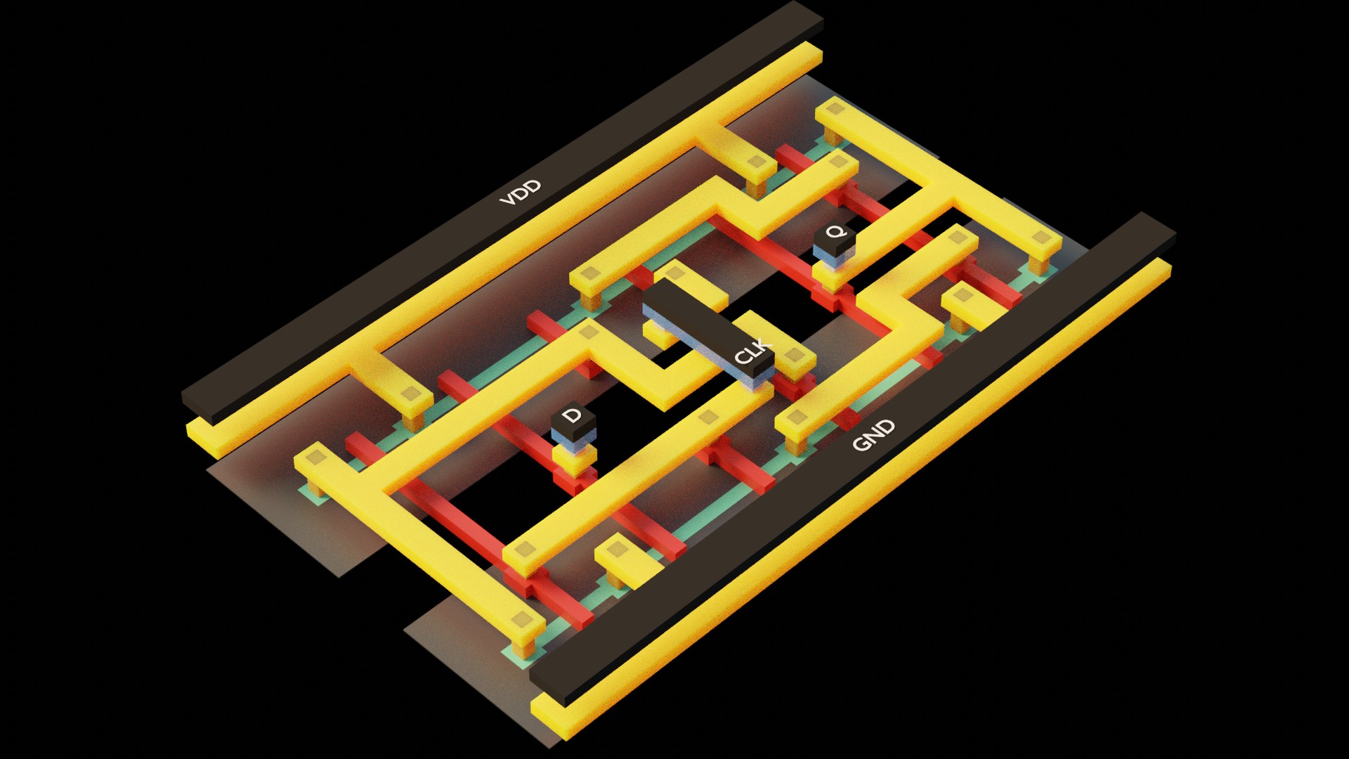
The development of the StdCellLib generator started in 2018, it is currently targeted for LS1U, Sky130 and GF180, and we did successful tapeouts on Sky130 already. We have prepared a library for GF180 for 5V already but haven’t taped it out yet.
Currently not yet in scope: Pad-Cells, but we hope to do that in the future, once the work on the standard cells is finished.
Test Structure Generator
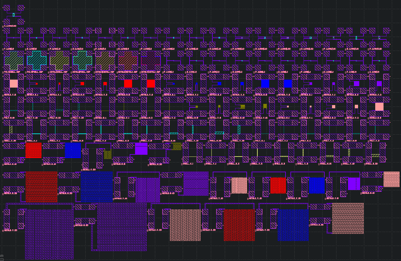
Test Structures are used to create Test-Chips with various carefully designed test structures on them which can then be measured to see and model the actual behavior of the chip production process. This can be used during process development to bring up a new process node, it can also be used to be placed on every wafer for quality assurance during production. It can also be used to additionally characterize an existing process node for new applications like new chemical layers like e.g. Hafnium, …
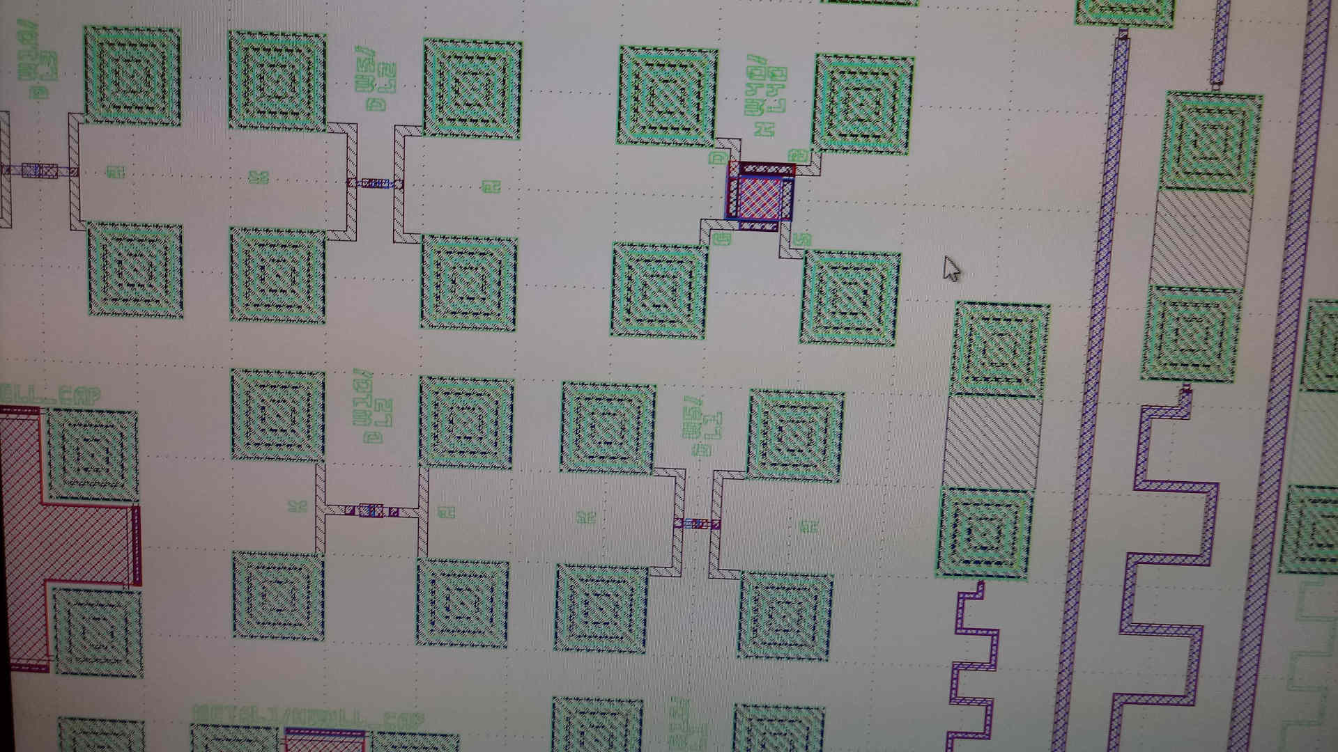
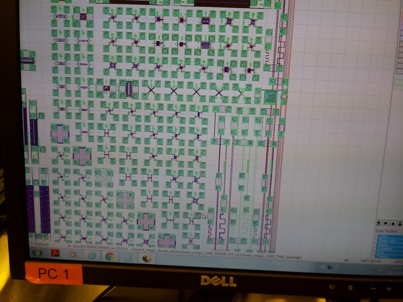
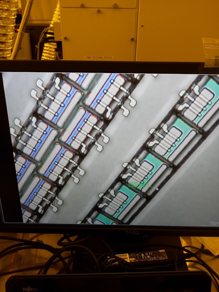
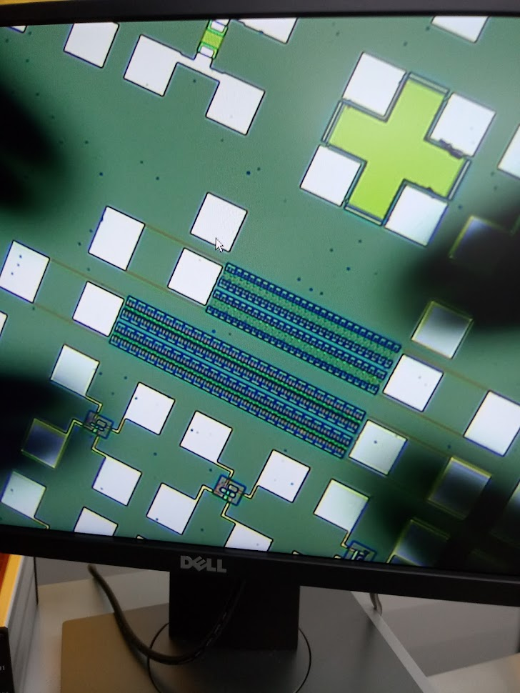
The initial project was the manually designed Pearl River for 1um process:

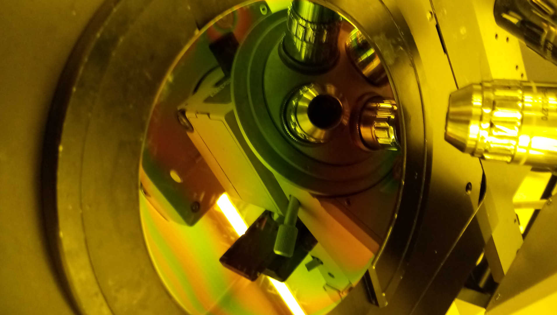
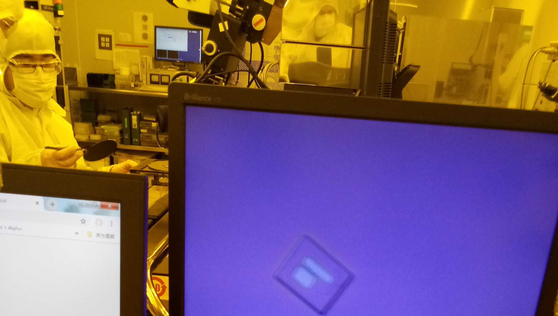
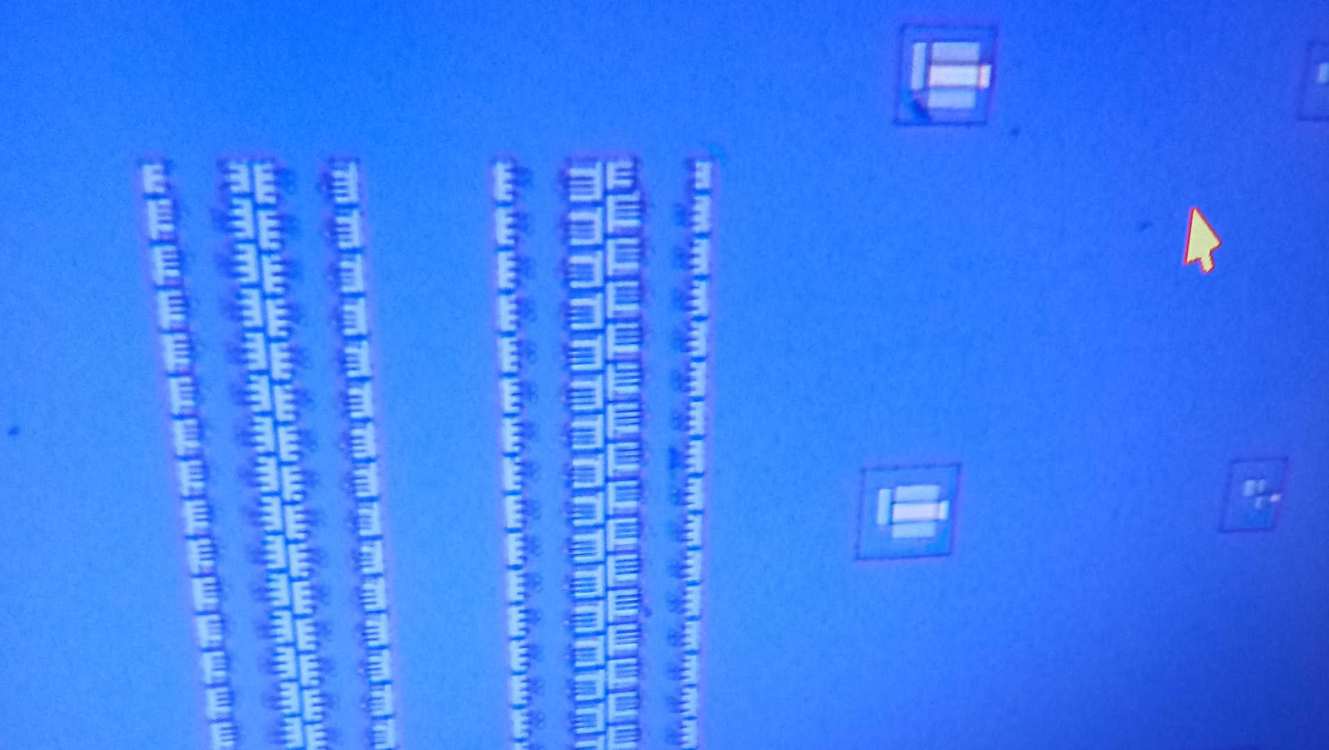
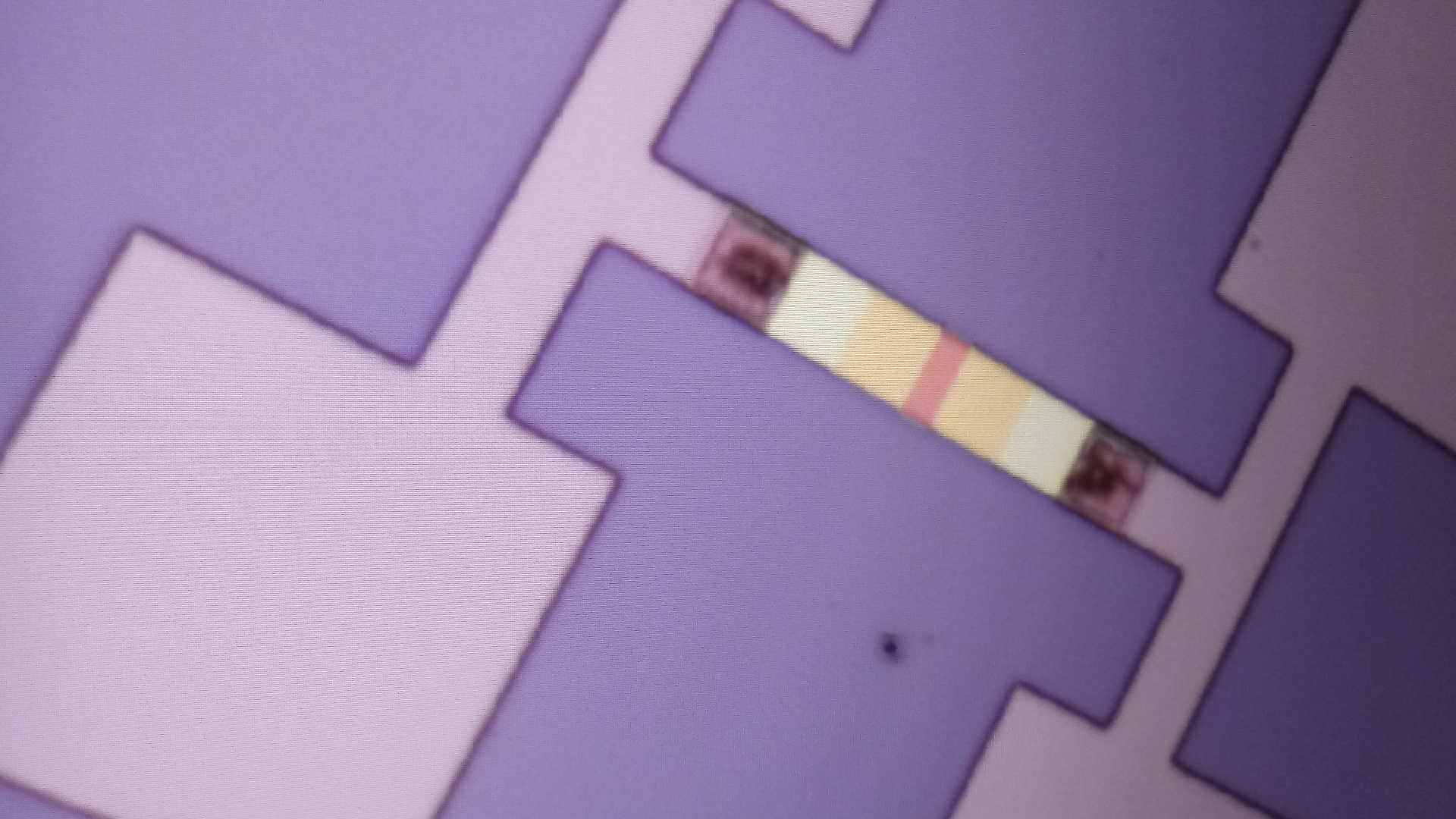
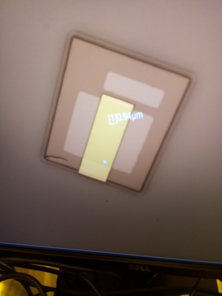
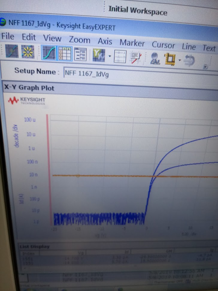
Pearl River was actually produced in the lab of HKUST in 2018 (Hong Kong University of Science and Technology) and transistors were tested successfully:
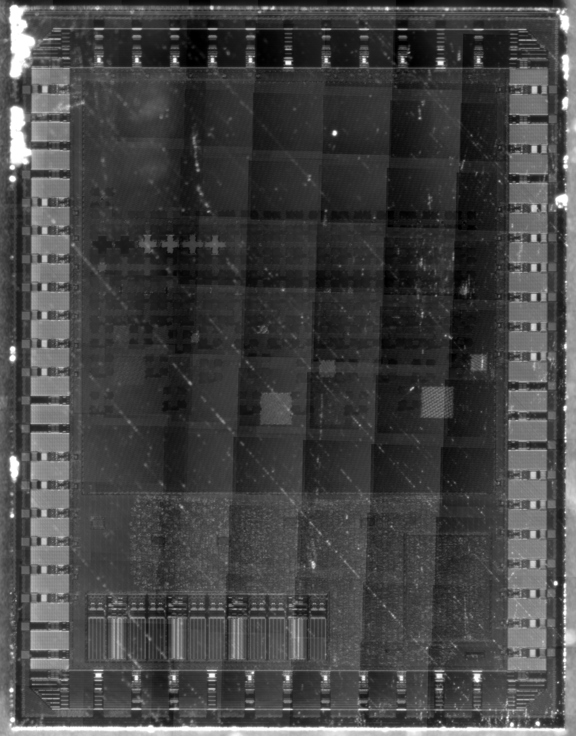
In 2023 we developed the automated successor, called DanubeRiver and taped it out successfully in cooperation with Google on GobalFoundries GF180.

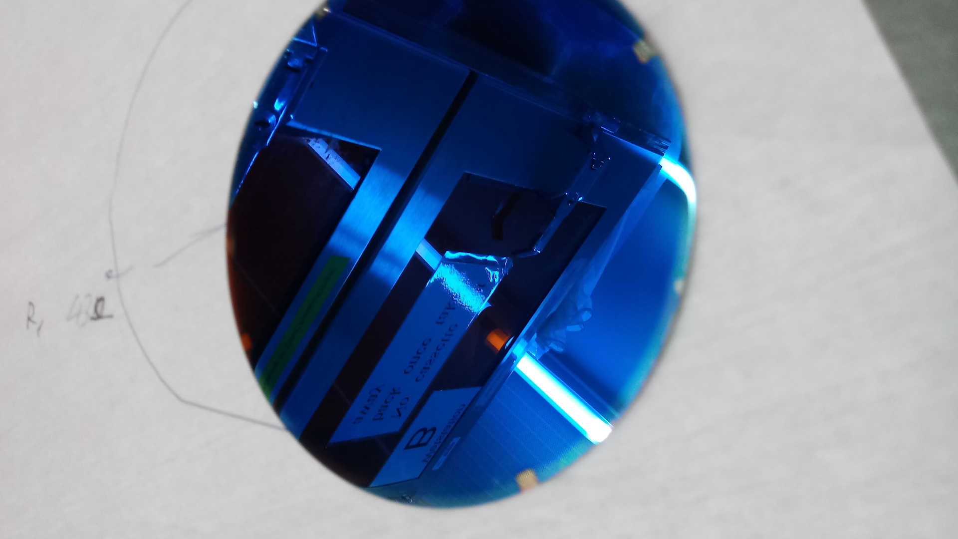
One of our GF180 test structure chips was successfully photographed by Andrew (“Bunnie”) Huang:

LibrePDK
LibrePDK is a software library which does parametric generation of structures, based on available design rules. It is used by DanubeRiver to create the teststructures, and it uses gdspy itself for generating GDS-II which is the data format used to transmit the chip design to the semiconductor factory.
LibrePDK was developed in 2022/2023
It has been successfully used in the GF180 tapeout for DanubeRiver.
LS1U - Libresilicon 1um Process Node
This is a fully open source, fully documented (process specifications, DRC rules, …) CMOS process design, with the goal that it should be adoptable by university labs and in the long run hobbyists.
The tests had started at HKUST, but were interrupted and haven’t been completed yet.
Several universities have adopted the process documentation in their lectures to teach CMOS manufacturing, e.g. JKU Linz (Austria).
The long term goal is to find alternative chemical recipes, which allow for private hobbyists to make their own chips without having to use very dangerous gasses like Silane, here is a not yet reliably verified alternative recipe for depositing Polysilicon for example: Eco friendly Polysilicon deposition_(CVD)
Our roadmap
The roadmap itself can be found here through the Roadmap Wiki Link
